Metal-oxide-semiconductor field-effect transistor
The Metal-oxide-semiconductor field-effect transistor (MOSFET) is a type of FET that consists of three layers: a metal top electrode (a conductor, called the gate), an oxide layer (working as an insulator separating the gate from the semiconductor layer), and a semiconductor layer (called the body). Its operation is based upon the modulation of the semiconductor conductivity by the electric field introduced in the body by the gate, the so-called field effect. This transistor was invented by Dawon Khang and Martin Atalla in 1960, at Bell Labs.[1]
There are four contacts altogether: in addition to the gate and body contacts already descirbed, there are two contacts atop the body at opposite sides of the gate called source and drain. Because the transistor is symmetrical, they can swap their functions. They do not permit current flow to the body in normal operation, as they form reverse biased diodes with the body. They do allow current between source and drain upon formation (by the gate) of a surface channel at the top surface of the body, next to the insulator. The channel conductivity depends upon the voltage difference between the gate and body (Vgb). The amount of current drawn in the channel depends upon the voltage drop across it, the drain to source voltage (Vds). The channel strength also is affected by so-called "back gate bias", that is, by the body to source voltage (Vbs).
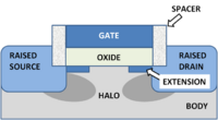
The modern MOSFET structure is shown in the figure (with a bow to artistic license). It is rather complex, as it is made to control a number of undesirable or parasitic effects that detract from its ideal behavior. Among these are unwanted capacitances between the gate and source and gate and drain, reduced by introduction of spacers at the sides of the gate. Another problem is high source-to-body and drain-to-body capacitance, which is reduced by raising the source and drain above the body, so the sidewall contact areas are reduced. These parasitic capacitances have to be charged and discharged between on and off conditions, and slow down device operation. Also undesired is penetration of the source and drain fields underneath the gate, which interferes with the channel formation. That effect is reduced by use of shallow junction extensions and screening halo implants, both designed to keep the source and drain fields close to their electrodes, and away from the gate.
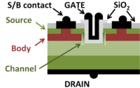
For power applications a different geometry is used, notably asymmetric in drain and source geometry. Special attention is given to the drain, which is adapted to large drain voltages. The figure shows an example called the UMOSFET because of the U-shaped gate. This cross-section is is only for one of a huge array of identical parallel fingers (the diagram is repeated to right and left with identical structures) all tied together in one device to handle large currents.[2] As indicated by different colors in the figure, the source and drain are both n-type, and the body is p-type, or vice versa. The drain is specially doped to have a wide drift region, allowing reduction of the large drain voltage before it reaches the channel, and also allowing the current from the channel to spread out before reaching the drain contact, lowering the device resistance.
History
Modern electronic circuits use the MOSFET.
In 1930, Julius Edgar Lilienfeld (1881-1963), from the University of Leipzig applied for a patent in which he described an element bearing resemblance to the MOS transistor and which could have been the first transistor in history. We had to wait until the 1960s in order to see the arrival of such devices, whose development was made possible with the resolution of many technical issues outlined below. Today, the MOS transistor is the key element of digital integrated circuits on a large scale and has led to the development of perhaps the most complex and sophisticated manufacturing enterprise on the planet.
A major obstacle that had to be overcome in realizing this device was the quality of the semiconductor-insulator interface, which in many materials systems contains a large number of interface traps that interfere with the field effect. It was found that the interface between silicon and silicon dioxide was close to ideal in this respect if care was taken in its preparation (a technique called surface passivation). A stability issue required removal of mobile ion contaminants from the oxide, notably sodium, which required careful control of all fabrication steps, and today is accomplished in manufacturing by controlled atmosphere clean rooms that keep all contaminants to very low levels never envisioned prior to manufacture of this device.[3] A major source of contaminants is the human body, so a modern "fab" requires operators to wear specially constructed bunny suits, with "booties", gowns, gloves, hair caps and masks.[4]
More recently, the challenges for MOSFET design are related to its miniaturization, a goal required by the modern integrated circuit that uses millions of these devices with dimensions in the range of tens of nm.[5] This miniaturization has led to entirely new fabrication methods, such as ion implantation to control dopant locations very accurately, sophisticated masking steps to construct tiny geometries,[6] and development of chemical procedures with rigid thermal budgets. This package of processes is sometimes called silicon planar technology.[7] The complexity of this processing and of circuits with millions of devices has led to development of computer-aided design involving sophisticated software that simulates everything from individual processes and devices to the layout of the entire circuit and the precise simulation of each step in its manufacture. The concepts of electronic design automation and design for manufacture are applied with mind-boggling rigor.[8]
Operation
A narrow, surface inversion layer of electrons forms at large enough positive gate voltages. The horizontal dashed line indicates the Fermi level that divides occupied energy levels from empty ones at zero temperature.
The control of the channel by the gate is similar to the formation of an inversion layer in the MOS capacitor, which is only a two-terminal device (gate and body contacts). The case of a p-type semiconductor body in which mobile holes are introduced in the valence band by introducing acceptor impurities is described below. The acceptors suck electrons out of the valence band, becoming fixed negative ions, and leaving electron vacancies in the valence band that behave as positively charge mobile holes.
The formation of this layer is understood by examining the behavior of the energy band edges under an applied field. The left-hand panels of the figure depict the lowest energy level of the conduction band of energies and the highest energy level of the valence band of energies (separated by the forbidden gap with no available energy levels) as a function of depth into the semiconductor body. In the figure's top panel, an applied voltage bends these band edges (left). This bending causes the valence band to become filled with electrons, so no holes are present. On the upper right, the figure shows the charge inducing this bending (Q) is balanced by a layer of negative acceptor-ion charge –QA in this depletion region where there are no holes. This depletion region of negative acceptor ions widens until neutrality is reached Q−QA = 0. In the bottom panel, a larger applied voltage further depletes holes from the surface but the conduction band becomes low enough in energy to populate with electrons near the surface, forming an inversion layer. The charge inducing the inversion layer is now balanced both by the inversion layer charge –Qn and by the depletion layer charge –QA, so now Q–Qn−QA = 0. Once the applied voltage is large enough to begin formation of the inversion layer, the charge balance is dominated by this layer, and the depletion region no longer expands significantly.
The electrons in the surface channel are mobile and form a conducting surface layer atop the insulating layer of fixed, immobile acceptor ions in the depletion region. The source and drain contacts on the body surface become connected by this conducting surface layer, so the formation of the inversion layer allows current to flow from the source to the drain. By contrast, when the conducting surface layer is not present, no conduction occurs, even when the surface layer is not depleted and holes are present. The contacts cannot conduct using holes because they are n-type semiconductor regions, and form pn-diode junctions with the body.
Thus, the source and drain are not electrically connected for voltages between zero and the threshold voltage for inversion layer formation. But once threshold voltage is exceeded, connection is established. The MOSFET constitutes an electrically controlled switch.
Two device types: n- and p-channel
The device above uses a p-type body and an electron inversion layer, or n-channel. In CMOS circuits these n-channel MOSFETs are combined with p-channel MOSFETs that use an n-type body and a hole inversion layer. These CMOS circuits consume low power as only the active devices in a sub-circuit (either the n-channel or the p-channel devices) are operational at a given time, and the complementary devices are "off".
Notes
- ↑ An historical run-down with references can be found in Gianfranco Cerofolini (2009). “Chapter 2: Top-down paradigm to miniaturization”, Nanoscale Devices: Fabrication, Functionalization, and Accessibility from the Macroscopic World. Springer, pp. 9 ff. ISBN 354092731X.
- ↑ B. Jayant Baliga (2010). “Chapter 3: U-MOSFET structure”, Advanced Power MOSFET Concepts. Springer, p. 66 ff. ISBN 1441959165.
- ↑ For a discussion, see Peter Van Zant (2004). “Chapter 5: Contamination control”, Microchip fabrication: a practical guide to semiconductor processing, 5th ed. McGraw-Hill, pp. 91 ff. ISBN 0071432418.
- ↑ See previously cited work Peter Van Zant. Microchip fabrication: a practical guide to semiconductor processing, pp. 112. ISBN 0071432418.
- ↑ A rule of thumb much used in the industry is Moore's law, which predicts a 20nm design rule will be realized in 2011. Already in mid-2010 initial fabrication had begun on the 22nm design node. See TSMC skips 22 nm, rolls 20-nm process. EE Times (4/13/2010). Retrieved on 2011-01-16.
- ↑ The techniques of microlithography involve a variety of masks and radiations that expose patterns that are then etched or "developed". See for example, J. Michael Köhler, Wolfgang Fritzsche (2007). “§3.4 Structure generation and fabrication of lithographic masks”, Nanotechnology: an introduction to nanostructuring techniques, 2nd ed. Wiley-VCH, p. 59. ISBN 3527318712.
- ↑ For a discussion, see for example, Chue San Yoo (2008). “§1.2 Evolution of integrated circuit industry”, Semiconductor manufacturing technology. World Scientific, pp. 5 ff. ISBN 9812568239.
- ↑ A selection of essays on these topics is found in (2006) Louis Scheffer: Electronic design automation for integrated circuits handbook, Volume 2. CRC Press. ISBN 0849379237.

