Thévenin's theorem
In the theory of electrical circuits, Thévenin's theorem allows the replacement of a two-terminal portion of a linear circuit by a simplified circuit consisting of a voltage source, called the Thévenin voltage source, in series with an impedance, called the Thévenin impedance. Thévenin's theorem is the dual of Norton's theorem, which replaces a two-terminal portion of a linear circuit by a simplified circuit consisting of a current source in parallel with an impedance.[1]
The upshot of using Thévenin's theorem is shown in the figure: the circuit behavior is boiled down to a simple voltage divider.
It will be noted that if the Thévenin impedance ZTh is much smaller than the original series driver resistance Zin, the output voltage across the load ZL benefits from a more favorable voltage division than occurs with direct attachment of the source to the load. In any event, the Thévenin circuit makes the voltage-division role of the complex circuit clear. In general, the Thévenin theorem is a tremendous aid to an intuitive understanding, essential for the creative design of circuits .
Finding the Thévenin components
To determine the Thévenin voltage, open circuit the two terminals and measure or calculate the open-circuit voltage across the terminals.
To determine the Thévenin impedance, set all independent sources between the two terminals to zero (leave the dependent sources active), and determine the impedance seen looking into the two terminals. For example, apply a known voltage across the port terminals and measure the current drawn, or apply a known current and determine the voltage developed. The Thévenin impedance is then the ratio of the voltage across the terminals to the current passing through the terminals.
In the case of a frequency dependent applied voltage or current, the impedance may be dependent upon frequency and exhibit a phase dependent upon frequency, as normally expressed using an impedance represented by a complex number.
Example
The bipolar circuit in the figure at left represents a voltage buffer. The operation of this circuit is as follows. The DC current source IE determines the current leaving the emitter in the quiescent state when no signal is applied. By appropriate selection of the DC current source it can be arranged that the transistor is configured to operate usefully, that is, it is in active mode.
A signal voltage vin is applied to the base. The emitter-to-base voltage of the transistor is hardly affected by the signal, and remains very nearly at the quiescent value determined by the bias current IE. Consequently as the signal changes the base voltage, the emitter voltage follows suit, and the output signal vout is a copy of the input signal vin. The DC current source does not permit any time varying current to pass through it, so at the signal frequency it behaves as an open circuit.
As this discussion indicates, the voltage gain of this circuit is very nearly unity, so amplification is not achieved. The purpose of this circuit is to isolate the signal source from the load RL, with the object of preventing the load from affecting the performance of the source. In particular, if the source is forced to draw a large current, that may adversely impact its performance, and this circuit insures that only a small current is demanded of the source. Because the object of this circuit is not voltage amplification, but isolation of the driver, it is called a voltage buffer.
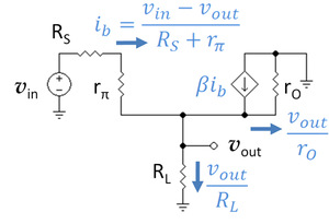
The transistor is a very nonlinear device, so the output signal voltage across the load resistor is not a faithful amplification of the input signal at the base unless the signal amplitude is small. For purposes of estimating the amplifier behavior, the assumption is made that the signal amplitudes are very small so the amplifier appears to behave as a linear circuit. Under these circumstances, the transistor can be approximated by a linear circuit composed of resistors called the hybrid pi model. The linear small-signal approximation to the circuit using the transistor hybrid pi model is shown in the figure with a few algebraic expressions derived by application of Ohm's law. This circuit is used to determine the Thévenin voltage (the open circuit voltage) of the buffer.
To apply this program, Kirchhoff's current law is applied to the emitter node in the upper small-signal circuit to obtain:
Inasmuch as β is a large number (perhaps 100 or more), the Thévenin voltage for this circuit is almost the same as the input voltage, the slightly smaller value being a result of the small variation of the base-emitter voltage of the transistor with the signal.
Of course, the load resistor RL should be allowed to become infinite to obtain an open-circuit condition, and the transistor output resistance is very large. Hence the validity of the approximate form.
To apply Thévenin's theorem, the resistance of the circuit looking back into the circuit from the output nodes is needed. That is accomplished using the second small-signal circuit. To determine the Thévenin impedance, the signal source is set to zero (short-circuited) and a test current ix is applied to the output and the resulting voltage at the output vx is determined. Applying Ohm's law to obtain the voltage drop across the series resistance rπ+RS, one finds:
where again, for an open-circuit condition RL should be allowed to become infinite, and as before ro is a large resistance, so the approximation is accurate.
Because the transistor β is typically more than 100, it can be seen that the Thévenin impedance is small in this circuit, and the the signal transferred to the load with the circuit in place will benefit from a favorable voltage division compared to direct attachment of the driver to the load.
References
- ↑ Adel S Sedra and Kenneth C Smith (1998). “Appendix E: Some useful network theorems”, Microelectronic circuits, 4rth ed. Oxford University Press, pp. E-1 ff. ISBN 0-19-511690-9.


