Hybrid-pi model
The hybrid-pi model is a popular circuit model used for analyzing the small signal behavior of transistors. The model can be quite accurate for low-frequency circuits and can easily be adapted for higher frequency circuits with the addition of appropriate inter-electrode capacitances and other parasitic elements.
Bipolar transistor
The hybrid-pi model is a linearized, y-parameter two-port network approximation to the transistor using the small-signal base-emitter voltage vπ and collector-emitter voltage vce as independent variables, and the small-signal base current ib and collector current ic as dependent variables. (See Jaeger and Blalock.[1])
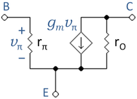
A basic, low-frequency hybrid-pi model for the bipolar transistor is shown in the figure. The three transistor terminals are E = emitter, B = base, and C = collector. The base-emitter connection is through a resistor rπ, and the base current causes a small-signal voltage drop across it, vπ (the π notation is standard). Voltage vπ induces a small-signal collector current via the voltage-controlled current source with current gmvπ, gm is the transistor transconductance.
The various parameters are as follows.
- is the transconductance in siemens, evaluated in a simple model (see Jaeger and Blalock[2])
- where:
- is the quiescent collector current (also called the collector bias or DC collector current)
- is the thermal voltage, calculated from Boltzmann's constant, the charge on an electron, and the transistor temperature in kelvins. At 290 K (an approximation to room temperature: 70°F ≈ 294 K) VT is very nearly 25 mV (Google calculator).
- in ohms
- where:
- is the current gain at low frequencies (commonly called hFE). Here is the Q-point base current. This is a parameter specific to each transistor, and can be found on a datasheet; is a function of the choice of collector current.
- is the output resistance due to the Early effect, and VA is called the Early voltage.
Higher frequencies
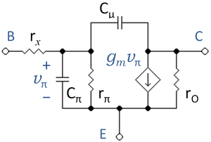
As frequencies are increased, amplifier gain drops off with increasing frequency because the bipolar transistor is degraded by parasitic capacitances. These effects must be modeled to assess the limitations of bipolar circuits. Three parasitic elements are commonly added to the hybrid-pi model to make frequency predictions. One is the base-emitter capacitance Cπ, which includes the base-emitter diffusion capacitance and the base-emitter junction capacitance. At high enough frequencies, Cπ shorts out the transistor and it fails to function. A second parasitic capacitance Cμ connects the base to the collector. Although this capacitor is small, its influence is multiplied by the transistor gain which amplifies the voltage variation at the base connection and applies it to the collector connection, exaggerating the influence of this capacitor through the Miller effect. The small series base resistance rx plays a role only when there is no other resistance introduced by the circuit into the base lead.
Related terms
The reciprocal of the output resistance is named the output conductance
- .
The reciprocal of gm is called the intrinsic resistance
- .
MOSFET parameters
Unlike the bipolar transistor, the MOSFET fundamentally is a four-terminal, not a three-terminal, device, the terminals being S = source, D = drain, G = gate, and B = body or substrate. The body is not normally used deliberately as a signal node, and the analogy to the bipolar device is stretched a bit to minimize differences between these devices.
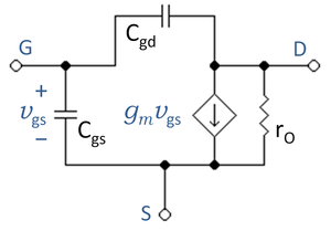
The upper figure shows the three-terminal small-signal equivalent circuit for the MOSFET, which ignores the body contact altogether. At low frequencies,the capacitances all are replaced with open circuits to obtain a frequency-independent circuit depending upon resistors only. The various parameters are as follows.
is the transconductance in siemens, evaluated in the Shichman-Hodges model in terms of the Q-point drain current by (see Jaeger and Blalock[3]):
- ,
- where:
- is the quiescent drain current (also called the drain bias or DC drain current)
- = threshold voltage and = gate-to-source voltage.
The combination:
often is called the overdrive voltage.
- is the output resistance due to channel length modulation, calculated using the Shichman-Hodges model as
- ,
using the approximation for the channel length modulation parameter λ[4]
- .
Here VE is a technology related parameter (about 4 V / μm for the 65 nm technology node[4]) and L is the length of the source-to-drain separation.
The reciprocal of the output resistance is named the drain conductance
- .
It must be pointed out that the Shichman-Hodges model has absolutely no claim to accuracy, especially in today's technology. However, it still is widely used in textbooks to get the flavor of MOSFET circuit design. Nobody would actually implement a circuit expecting this model to be quantitative, however, and real design work always involves extensive computer modeling, for example, using the BSIM computer model.[5]
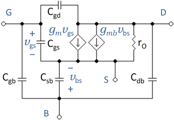
The lower figure explicitly introduces the body contact and the capacitances to the body. This circuit is a great deal more complicated than the three-terminal circuit, and is avoided where possible. However, in some circuits the body is not held at signal ground, and the body must be explicitly handled.
References and notes
- ↑ R.C. Jaeger and T.N. Blalock (2004). Microelectronic Circuit Design, Second Edition. New York: McGraw-Hill, Section 13.5, esp. Eqs. 13.19. ISBN 0-07-232099-0.
- ↑ R.C. Jaeger and T.N. Blalock. Eq. 5.45 pp. 242 and Eq. 13.25 p. 682. ISBN 0-07-232099-0.
- ↑ R.C. Jaeger and T.N. Blalock. Eq. 4.20 pp. 155 and Eq. 13.74 p. 702. ISBN 0-07-232099-0.
- ↑ 4.0 4.1 W. M. C. Sansen (2006). Analog Design Essentials. Dordrechtμ: Springer. ISBN 0-387-25746-2.
- ↑ A popular MOSFET computer model is BSIM4, see: BSIM4.6.4 MOSFET Model: User's manual. BSIM 4 web site. Electrical Engineering and Computer Sciences Department, UC Berkeley (2009). Retrieved on 2011-05-20. This 170-page manual describes a model much more complex than a simple algebraic formula.


