imported>John R. Brews |
|
| (103 intermediate revisions by one other user not shown) |
| Line 1: |
Line 1: |
| | {{AccountNotLive}} |
| {{TOC|right}} | | {{TOC|right}} |
| | [[Image:Current division example.svg|thumbnail|250px|Figure 1: Schematic of an electrical circuit illustrating current division. Notation ''R<sub>T<sub>.</sub></sub>'' refers to the ''total'' resistance of the circuit to the right of resistor ''R<sub>X</sub>''.]] |
|
| |
|
| {{Image|Two-port with Thevenin driver.PNG|right|350px| Two-port network with symbol definitions. A [[Thevenin voltage source]] with [[Thevenin impedance]] ''Z<sub>Th</sub>'' drives port 1, and impedance ''Z<sub>L</sub>'' loads port 2}}
| | In [[electronics]], a '''current divider ''' is a simple [[linear]] [[Electrical network|circuit]] that produces an output [[Electric current|current]] (''I''<sub>X</sub>) that is a fraction of its input current (''I''<sub>T</sub>). The splitting of current between the branches of the divider is called '''current division'''. The currents in the various branches of such a circuit divide in such a way as to minimize the total energy expended. |
| A '''two-port network''' is an [[electrical circuit]] with two ''pairs'' of terminals. As shown in the figure, two terminals constitute a '''port''' ''only'' if they satisfy the essential requirement known as the '''port condition''', namely, the same current must enter and leave a port.<ref name=Gray/><ref name=Jaeger/>
| |
| Examples include small-signal models for transistors (such as the [[hybrid-pi model]]), [[electronic filter|filter]]s and [[matching network]]s. The analysis of passive two-port networks is an outgrowth of reciprocity theorems first derived by Lorentz.<ref name=Jasper/>
| |
|
| |
|
| A two-port network makes possible the replacement of either a complete circuit or part of it by a "[[black box]]" with a only four distinct parameters, enabling us to separate its behavior from that of its internal constituents, thus simplifying analysis. Any linear circuit with four terminals can be transformed into a two-port network provided that it does not contain an independent source and satisfies the port conditions.
| | The formula describing a current divider is similar in form to that for the [[voltage divider]]. However, the ratio describing current division places the impedance of the unconsidered branches in the [[numerator]], unlike voltage division where the considered impedance is in the numerator. To be specific, if two or more [[Electrical impedance|impedance]]s are in parallel, the current that enters the combination will be split between them in inverse proportion to their impedances (according to [[Ohm's law]]). It also follows that if the impedances have the same value the current is split equally. |
|
| |
|
| The parameters used to describe a two-port network are the following: z, y, h, g. Each choice corresponds to a different choice for which pair of variables from port 1 and port 2 are chosen to be independent, externally applied sources and which two will be the dependent resultant variables determine by the two-port parameters (see the figure). The port currents and voltages are denoted as follows:
| | ==Resistive divider== |
| :<math>{V_1}</math> = Port 1 voltage | | A general formula for the current ''I<sub>X</sub>'' in a resistor ''R<sub>X</sub>'' that is in parallel with a combination of other resistors of total resistance ''R<sub>T</sub>'' is (see Figure 1): |
| :<math>{I_1}</math> = Port 1 current
| | :<math>I_X = \frac{R_T}{R_X+R_T}I_T \ </math> |
| :<math>{V_2}</math> = Port 2 voltage
| | where ''I<sub>T</sub>'' is the total current entering the combined network of ''R<sub>X</sub>'' in parallel with ''R<sub>T</sub>''. Notice that when ''R<sub>T</sub>'' is composed of a [[Series_and_parallel_circuits#Parallel_circuits|parallel combination]] of resistors, say ''R<sub>1</sub>'', ''R<sub>2</sub>'', ... ''etc.'', then the reciprocal of each resistor must be added to find the total resistance ''R<sub>T</sub>'': |
| :<math>{I_2}</math> = Port 2 current | | :<math> \frac {1}{R_T} = \frac {1} {R_1} + \frac {1} {R_2} + \frac {1}{R_3} + ... \ . </math> |
| The relations between inputs and outputs usually are expressed in matrix notation.
| |
|
| |
|
| These variables are most useful at low to moderate frequencies. At high frequencies (for example, microwave frequencies) power and energy are more useful variables, and the two-port approach based on current and voltages that is discussed here is replaced by an approach based upon [[scattering parameters]].<ref name=Pozar/>
| | ==General case== |
| | Although the resistive divider is most common, the current divider may be made of frequency dependent [[Electrical impedance|impedance]]s. In the general case the current I<sub>X</sub> is given by: |
| | :<math>I_X = \frac{Z_T} {Z_X+Z_T}I_T \ ,</math> |
|
| |
|
| Though some authors use the terms ''two-port network'' and ''four-terminal network'' interchangeably, the latter represents a more general concept. '''Not all four-terminal networks are two-port networks.''' A pair of terminals can be called a ''port'' only if the current entering one is equal to the current leaving the other (the '''port condition'''). Only those four-terminal networks in which the four terminals can be paired into two ports can be called two-ports.<ref name=Gray/><ref name=Jaeger/>
| | ==Using Admittance== |
| | Instead of using [[Electrical impedance|impedance]]s, the current divider rule can be applied just like the [[voltage divider]] rule if [[admittance]] (the inverse of impedance) is used. |
| | :<math>I_X = \frac{Y_X} {Y_{Total}}I_T</math> |
| | Take care to note that Y<sub>Total</sub> is a straightforward addition, not the sum of the inverses inverted (as you would do for a standard parallel resistive network). For Figure 1, the current I<sub>X</sub> would be |
| | :<math>I_X = \frac{Y_X} {Y_{Total}}I_T = \frac{\frac{1}{R_X}} {\frac{1}{R_X} + \frac{1}{R_1} + \frac{1}{R_2} + \frac{1}{R_3}}I_T</math> |
|
| |
|
| == Impedance parameters (z-parameters)== | | ===Example: RC combination=== |
| {{Image|Z-equivalent two-port.PNG|right|350px| Z-equivalent two port showing independent variables ''I<sub>1</sub>'' and ''I<sub>2</sub>''.}}
| | [[Image:Low pass RC filter.PNG|thumbnail|220px|Figure 2: A low pass RC current divider]] |
| The figure shows the two-port driven by two external current sources, making the input currents ''I<sub>1</sub>'' and ''I<sub>2</sub>'' the independent variables controlled from outside the two-port. The port voltages are determined in terms of these input currents by the ''z''-parameters defined by:
| | Figure 2 shows a simple current divider made up of a [[capacitor]] and a resistor. Using the formula above, the current in the resistor is given by: |
| :<math> \left[ \begin{array}{c} V_1 \\ V_2 \end{array} \right] = \left[ \begin{array}{cc} z_{11} & z_{12} \\ z_{21} & z_{22} \end{array} \right] \left[ \begin{array}{c}I_1 \\ I_2 \end{array} \right] </math>.
| |
|
| |
|
| :<math>z_{11} = {V_1 \over I_1 } \bigg|_{I_2 = 0} \qquad z_{12} = {V_1 \over I_2 } \bigg|_{I_1 = 0}</math> | | ::<math> I_R = \frac {\frac{1}{j \omega C}} {R + \frac{1}{j \omega C} }I_T </math> |
| | :::<math> = \frac {1} {1+j \omega CR} I_T \ , </math> |
| | where ''Z<sub>C</sub> = 1/(jωC) '' is the impedance of the capacitor. |
|
| |
|
| :<math>z_{21} = {V_2 \over I_1 } \bigg|_{I_2 = 0} \qquad z_{22} = {V_2 \over I_2 } \bigg|_{I_1 = 0}</math>
| | The product ''τ = CR'' is known as the [[time constant]] of the circuit, and the frequency for which ωCR = 1 is called the [[corner frequency]] of the circuit. Because the capacitor has zero impedance at high frequencies and infinite impedance at low frequencies, the current in the resistor remains at its DC value ''I<sub>T</sub>'' for frequencies up to the corner frequency, whereupon it drops toward zero for higher frequencies as the capacitor effectively [[short-circuit]]s the resistor. In other words, the current divider is a [[low pass filter]] for current in the resistor. |
|
| |
|
| Notice that all the series connected elements represented by z-parameters have dimensions of ohms, as do the dependent source parameters.
| | ==Loading effect== |
| | [[Image:Current division.PNG|thumbnail|300px|Figure 3: A current amplifier (gray box) driven by a Norton source (''i<sub>S</sub>'', ''R<sub>S</sub>'') and with a resistor load ''R<sub>L</sub>''. Current divider in blue box at input (''R<sub>S</sub>'',''R<sub>in</sub>'') reduces the current gain, as does the current divider in green box at the output (''R<sub>out</sub>'',''R<sub>L</sub>'')]] |
| | The gain of an amplifier generally depends on its source and load terminations. Current amplifiers and transconductance amplifiers are characterized by a short-circuit output condition, and current amplifiers and transresistance amplifiers are characterized using ideal infinite impedance current sources. When an amplifier is terminated by a finite, non-zero termination, and/or driven by a non-ideal source, the effective gain is reduced due to the '''loading effect''' at the output and/or the input, which can be understood in terms of current division. |
|
| |
|
| ===Example: bipolar [[current mirror]] with emitter degeneration===
| | Figure 3 shows a current amplifier example. The amplifier (gray box) has input resistance ''R<sub>in</sub>'' and output resistance ''R<sub>out</sub>'' and an ideal current gain ''A<sub>i</sub>''. With an ideal current driver (infinite Norton resistance) all the source current ''i<sub>S</sub>'' becomes input current to the amplifier. However, for a [[Norton's theorem|Norton driver]] a current divider is formed at the input that reduces the input current to |
| {{Image|Bipolar current mirror with emitter resistors.PNG|left|200px| Bipolar current mirror: ''I<sub>1</sub>'' is the ''reference current'' and ''I<sub>2</sub>'' is the ''output current''.}}
| |
| {{Image|Small-signal circuit for bipolar mirror.PNG|right|300px| Small-signal circuit for bipolar current mirror: ''I<sub>1</sub>'' is the amplitude of the small-signal ''reference current'' and ''I<sub>2</sub>'' is the amplitude of the small-signal ''output current''.}}
| |
| The figure at left shows a bipolar current mirror with emitter resistors to increase its output resistance.<ref name=feedback/> Transistor ''Q<sub>1</sub>'' is ''diode connected'', which is to say its collector-base voltage is zero. The figure at right shows the small-signal circuit equivalent to the transistor circuit. Transistor ''Q<sub>1</sub>'' is represented by its emitter resistance ''r<sub>E</sub>'' ≈ ''V<sub>T</sub> / I<sub>E</sub>'' (''V<sub>T</sub>'' = thermal voltage, ''I<sub>E</sub>'' = [[Q-point]] emitter current), a simplification made possible because the dependent current source in the hybrid-pi model for ''Q<sub>1</sub>'' draws the same current as a resistor 1 / ''g<sub>m</sub>'' connected across ''r<sub>π</sub>''. The second transistor ''Q<sub>2</sub>'' is represented by its [[hybrid-pi model]]. Table 1 below shows the z-parameter expressions that make the z-equivalent two-port electrically equivalent to the small-signal circuit for the mirror.
| |
| {| class="wikitable" style="background:white;text-align:center;margin: 1em auto 1em auto"
| |
| !Table 1 !! Expression !! Approximation
| |
|
| |
|
| |-valign="center"
| | ::<math>i_{i} = \frac {R_S} {R_S+R_{in}} i_S \ , </math> |
| |<math>R_{21} = \begin{matrix} {V_\mathrm{2} \over I_\mathrm{1} }\end{matrix} \Big|_{I_{2}=0} </math>
| |
| |<math> - ( \beta r_O - R_E ) </math> <math> \begin{matrix} \frac {r_E +R_E }{r_{ \pi}+r_E +2R_E} \end{matrix} </math>
| |
| |<math> - \beta r_o </math><math> \begin{matrix} \frac {r_E+R_E }{r_{ \pi} +2R_E}\end{matrix} </math>
| |
|
| |
|
| |-valign="center"
| | which clearly is less than ''i<sub>S</sub>''. Likewise, for a short circuit at the output, the amplifier delivers an output current ''i<sub>o</sub>'' = ''A<sub>i</sub> i<sub>i</sub>'' to the short-circuit. However, when the load is a non-zero resistor ''R<sub>L</sub>'', the current delivered to the load is reduced by current division to the value: |
| |<math>R_{11}= \begin{matrix} \frac{V_{1}}{I_{1}}\end{matrix} \Big|_{I_{2}=0} </math>
| |
| |<math> (r_E + R_E)</math> <math>// </math> <math>(r_{ \pi} +R_E) </math>
| |
| |<math></math>
| |
|
| |
|
| |-valign="center"
| | ::<math>i_L = \frac {R_{out}} {R_{out}+R_{L}} A_i i_{i} \ . </math> |
| |<math> R_{22} = \begin{matrix} \frac{V_{2}}{I_{2}}\end{matrix} \Big|_{I_{1}=0} </math>
| |
| |<math> \ ( </math><math> 1 + \beta </math> <math> \begin{matrix} \frac {R_E} {r_{ \pi} +r_E+2R_E } \end{matrix} ) </math> <math> r_O </math> <math>+ \begin{matrix} \frac { r_{ \pi}+r_E +R_E }{r_{ \pi}+r_E +2R_E } \end{matrix} </math><math>R_E</math>
| |
| |<math> \ ( </math><math>1 + \beta </math><math> \begin{matrix} \frac {R_E} {r_{ \pi}+2R_E } \end{matrix} ) </math> <math>r_O </math>
| |
|
| |
|
| |-valign="center"
| | Combining these results, the ideal current gain ''A<sub>i</sub>'' realized with an ideal driver and a short-circuit load is reduced to the '''loaded gain''' ''A<sub>loaded</sub>'': |
| |<math> R_{12} = \begin{matrix} {V_\mathrm{1} \over I_\mathrm{2} }\end{matrix} \Big|_{I_{1}=0} </math>
| |
| |<math>R_E </math> <math>\begin{matrix} \frac {r_E+R_E} {r_{ \pi} +r_E +2R_E} \end{matrix}</math>
| |
| |<math>R_E</math> <math> \begin{matrix} \frac {r_E+R_E} {r_{ \pi} +2R_E} \end{matrix}</math>
| |
| |}
| |
|
| |
|
| The negative feedback introduced by resistors ''R<sub>E</sub>'' can be seen in these parameters. For example, when used as an active load in a differential amplifier, ''I<sub>1</sub> ≈ -I<sub>2</sub>'', making the output impedance of the mirror approximately ''R<sub>22</sub> -R<sub>21</sub>'' ≈ 2 β ''r<sub>O</sub>R<sub>E</sub>'' /( ''r<sub>π</sub>+2R<sub>E</sub>'' ) compared to only ''r<sub>O</sub>'' without feedback (that is with ''R<sub>E</sub>'' = 0 Ω) . At the same time, the impedance on the reference side of the mirror is approximately ''R<sub>11</sub> -R<sub>12</sub>'' ≈ <math> \begin{matrix} \frac {r_{\pi}} {r_{\pi}+2R_E} \end{matrix} </math> <math> (r_E+R_E)</math>, only a moderate value, but still larger than ''r<sub>E</sub>'' with no feedback. In the differential amplifier application, a large output resistance increases the difference-mode gain, a good thing, and a small mirror input resistance is desirable to avoid [[Miller effect]].
| | ::<math>A_{loaded} =\frac {i_L} {i_S} = \frac {R_S} {R_S+R_{in}}</math> <math> \frac {R_{out}} {R_{out}+R_{L}} A_i \ . </math> |
|
| |
|
| ==Admittance parameters (y-parameters) ==
| | The resistor ratios in the above expression are called the '''loading factors'''. For more discussion of loading in other amplifier types, see [[Voltage division#Loading effect|loading effect]]. |
| {{Image|Y-equivalent two-port.PNG|right|350px| Y-equivalent two port showing independent variables ''V<sub>1</sub>'' and ''V<sub>2</sub>''.}}
| |
| The figure shows the two-port driven by two external voltage sources, making the input voltages ''V<sub>1</sub>'' and ''V<sub>2</sub>'' the independent variables controlled from outside the two-port. The port currents are determined in terms of these input voltages by the ''y''-parameters defined by: | |
|
| |
|
| :<math> \left[ \begin{array}{c} I_1 \\ I_2 \end{array} \right] = \left[ \begin{array}{cc} y_{11} & y_{12} \\ y_{21} & y_{22} \end{array} \right] \left[ \begin{array}{c}V_1 \\ V_2 \end{array} \right] </math>. | | ===Unilateral versus bilateral amplifiers=== |
| | [[Image:H-parameter current amplifier.PNG|thumbnail|300px|Figure 4: Current amplifier as a bilateral two-port network; feedback through dependent voltage source of gain β V/V]] |
| | Figure 3 and the associated discussion refers to a [[Electronic amplifier#Unilateral or bilateral|unilateral]] amplifier. In a more general case where the amplifier is represented by a [[two-port network|two port]], the input resistance of the amplifier depends on its load, and the output resistance on the source impedance. The loading factors in these cases must employ the true amplifier impedances including these bilateral effects. For example, taking the unilateral current amplifier of Figure 3, the corresponding bilateral two-port network is shown in Figure 4 based upon [[Two-port network#Hybrid parameters (h-parameters)| h-parameters]].<ref name=H_port/> Carrying out the analysis for this circuit, the current gain with feedback ''A<sub>fb</sub>'' is found to be |
|
| |
|
| where
| | ::<math> A_{fb} = \frac {i_L}{i_S} = \frac {A_{loaded}} {1+ {\beta}(R_L/R_S) A_{loaded}} \ . </math> |
|
| |
|
| :<math>y_{11} = {I_1 \over V_1 } \bigg|_{V_2 = 0} \qquad y_{12} = {I_1 \over V_2 } \bigg|_{V_1 = 0}</math>
| | That is, the ideal current gain ''A<sub>i</sub>'' is reduced not only by the loading factors, but due to the bilateral nature of the two-port by an additional factor<ref>Often called the ''improvement factor'' or the ''desensitivity factor''.</ref> ( 1 + β (R<sub>L</sub> / R<sub>S</sub> ) A<sub>loaded</sub> ), which is typical of [[negative feedback amplifier]] circuits. The factor β (R<sub>L</sub> / R<sub>S</sub> ) is the current feedback provided by the voltage feedback source of voltage gain β V/V. For instance, for an ideal current source with ''R<sub>S</sub>'' = ∞ Ω, the voltage feedback has no influence, and for ''R<sub>L</sub>'' = 0 Ω, there is zero load voltage, again disabling the feedback. |
|
| |
|
| :<math>y_{21} = {I_2 \over V_1 } \bigg|_{V_2 = 0} \qquad y_{22} = {I_2 \over V_2 } \bigg|_{V_1 = 0}</math>
| | ==References and notes== |
| | |
| | |
| The network is said to be reciprocal if <math> y_{12} = y_{21}</math>. Notice that all the shunt-connected elements are represented by y-parameters with dimensions of siemens, as are the dependent source parameters.
| |
| | |
| ==Hybrid parameters (h-parameters) ==
| |
| {{Image|H-equivalent two-port.PNG|right|350px|H-equivalent two-port showing independent variables ''I<sub>1</sub>'' and ''V<sub>2</sub>''.}}
| |
| The figure shows the two-port driven by two external sources, a current source at port 1 and a voltage source at port 2, making the input current ''I<sub>1</sub>'' and input voltage ''V<sub>2</sub>'' the independent variables controlled from outside the two-port. The voltage at port 1, ''V<sub>1</sub>'', and the current at port 2, ''I<sub>2</sub>'', are determined in terms of these inputs by the ''h''-parameters defined by:
| |
| :<math> {V_1 \choose I_2} = \begin{pmatrix} h_{11} & h_{12} \\ h_{21} & h_{22} \end{pmatrix}{I_1 \choose V_2} </math>.
| |
| | |
| where
| |
| | |
| :<math>h_{11} = {V_1 \over I_1 } \bigg|_{V_2 = 0} \qquad h_{12} = {V_1 \over V_2 } \bigg|_{I_1 = 0}</math>
| |
| | |
| :<math>h_{21} = {I_2 \over I_1 } \bigg|_{V_2 = 0} \qquad h_{22} = {I_2 \over V_2 } \bigg|_{I_1 = 0}</math>
| |
| | |
| Often this circuit is selected when a current amplifier is described, because the port 1 input is the independent input current and port 2 output is the dependent current.
| |
| | |
| Notice that off-diagonal h-parameters are dimensionless, while the series-connected diagonal element has dimensions of ohms, while the shunt-connected diagonal element has dimensions of siemens.
| |
| | |
| ===Example: common base amplifier===
| |
| {{Image|Common base with current drive.PNG|left|200px|Common base circuit with active load and current drive.}}
| |
| {{Image|Common base with current driver.PNG|right|300px|Common-base amplifier with AC current source ''I<sub>1</sub>'' as signal input and unspecified load supporting voltage ''V<sub>2</sub>'' and a dependent current ''I<sub>2</sub>''.}}
| |
| The common base amplifier is shown at left. The signal voltage is applied to the emitter, and output signal is taken from the collector. The current source in the collector lead is an ideal DC source, and as such will not allow passage of any varying signal through itself. Its purpose in the circuit is to proved a DC bias current that sets the operating point (the quiescent transistor state about which the transistor varies in processing the signal). The output node is shown as an open circuit (no load) at the left, but to make use of the amplifier, a load can be attached, which then will draw a signal current from the collector node.
| |
| | |
| The small-signal circuit at the right assumes the voltage at the collector is a specified variable, and the output current is to be determined. The input current at the emitter also is a specified variable, and the signal voltage developed at the emitter is a dependent variable.
| |
| | |
| Tabulated formulas in Table 2 make the h-equivalent circuit of the transistor agree with the small-signal low-frequency circuit found using the transistor [[hybrid-pi model]] at the right. Notation: ''r<sub>π</sub>'' = base resistance of transistor, ''r<sub>O</sub>'' = output resistance, and ''g<sub>m</sub>'' = transconductance. The negative sign for ''h<sub>21</sub>'' reflects the convention that ''I<sub>1</sub>'', ''I<sub>2</sub>'' are positive when directed ''into'' the two-port. A non-zero value for ''h<sub>12</sub>'' means the output voltage affects the input voltage, that is, this amplifier is '''bilateral'''. If ''h<sub>12</sub>'' = 0, the amplifier is '''unilateral'''.
| |
| | |
| {| class="wikitable" style="background:white;text-align:center;margin: 1em auto 1em auto"
| |
| !Table 2 !! Expression !! Approximation
| |
| | |
| |-valign="center"
| |
| |<math>h_{21} = \begin{matrix} {I_\mathrm{2} \over I_\mathrm{1} }\end{matrix} \Big|_{V_{2}=0} </math>
| |
| |<math> \begin{matrix} - \frac {\frac {\beta }{\beta+1}r_O +r_E} {r_O+r_E} \end{matrix} </math>
| |
| |<math>\begin{matrix} - \frac {\beta }{\beta+1}\end{matrix} </math>
| |
| | |
| |-valign="center"
| |
| |<math>h_{11}= \begin{matrix} \frac{V_{1}}{I_{1}}\end{matrix} \Big|_{V_{2}=0} </math>
| |
| |<math> r_E//r_O </math>
| |
| |<math>r_E</math>
| |
| | |
| |-valign="center"
| |
| |<math> h_{22} = \begin{matrix} \frac{I_{2}}{V_{2}}\end{matrix} \Big|_{I_{1}=0} </math>
| |
| |<math> \begin{matrix} \frac {1} {( \beta +1) ( r_O +r_E)} \end{matrix} </math>
| |
| |<math> \begin{matrix} \frac {1} {( \beta +1) r_O } \end{matrix} </math>
| |
| | |
| |-valign="center"
| |
| |<math> h_{12} = \begin{matrix} {V_\mathrm{1} \over V_\mathrm{2} }\end{matrix} \Big|_{I_{1}=0} </math>
| |
| |<math>\ \begin{matrix} \frac {r_E} {r_E+r_O} \end{matrix} \ </math>
| |
| |<math>\ \begin{matrix} \frac {r_E} {r_O} \end{matrix} \ </math> << 1
| |
| |}
| |
| | |
| ==Inverse hybrid parameters (g-parameters)==
| |
| {{Image|G-equivalent two-port.PNG|right|350px| G-equivalent two-port showing independent variables ''V<sub>1</sub>'' and ''I<sub>2</sub>''.}}
| |
| The figure shows the two-port driven by two external sources, a voltage source at port 1 and a current source at port 2, making the input voltage ''V<sub>1</sub>'' and input current ''I<sub>2</sub>'' the independent variables controlled from outside the two-port. The current at port 1, ''I<sub>1</sub>'', and the voltage at port 2, ''V<sub>2</sub>'', are determined in terms of these inputs by the ''g''-parameters defined by:
| |
| | |
| :<math> {I_1 \choose V_2} = \begin{pmatrix} g_{11} & g_{12} \\ g_{21} & g_{22} \end{pmatrix}{V_1 \choose I_2} </math>.
| |
| | |
| where
| |
| | |
| :<math>g_{11} = {I_1 \over V_1 } \bigg|_{I_2 = 0} \qquad g_{12} = {I_1 \over I_2 } \bigg|_{V_1 = 0}</math>
| |
| | |
| :<math>g_{21} = {V_2 \over V_1 } \bigg|_{I_2 = 0} \qquad g_{22} = {V_2 \over I_2 } \bigg|_{V_1 = 0}</math>
| |
| | |
| | |
| Often this circuit is selected to describe a voltage amplifier, as the port 1 input is an independent voltage, and the port 2 output is a dependent voltage. Notice that off-diagonal g-parameters are dimensionless, while the series-connected diagonal element has dimensions of ohms, while the shunt-connected diagonal element has dimensions of siemens.
| |
| | |
| ===Example: [[common base]] amplifier===
| |
| {{Image|Common base with voltage drive.PNG|left|200px|Bipolar transistor with base grounded and signal applied to emitter.}}
| |
| {{Image|Small-signal common base circuit.PNG|right|300px|Common-base amplifier with AC voltage source ''V<sub>1</sub>'' as signal input and unspecified load delivering current ''I<sub>2</sub>'' at a dependent voltage ''V<sub>2</sub>''.}}
| |
| The common base amplifier is shown again at the left. This time, a signal ''voltage'' is applied to the emitter, and an output ''current'' is taken from the collector.
| |
| | |
| The small-signal circuit at the right assumes the current at the collector is a specified variable, and the output voltage is to be determined. The input voltage at the emitter also is a specified variable, and the signal current driven into the emitter is a dependent variable.
| |
| | |
| The tabulated formulas in Table 3 make the g-equivalent two-port for the amplifier agree with the small-signal circuit found using the small-signal low-frequency [[hybrid-pi model]] for the transistor. Notation: ''r<sub>π</sub>'' = base resistance of transistor, ''r<sub>O</sub>'' = output resistance, and ''g<sub>m</sub>'' = transconductance. The negative sign for ''g<sub>12</sub>'' reflects the convention that ''I<sub>1</sub>'', ''I<sub>2</sub>'' are positive when directed ''into'' the two-port. A non-zero value for ''g<sub>12</sub>'' means the output current affects the input current, that is, this amplifier is '''bilateral'''. If ''g<sub>12</sub>'' = 0, the amplifier is '''unilateral'''.
| |
| | |
| {| class="wikitable" style="background:white;text-align:center;margin: 1em auto 1em auto"
| |
| !Table 3 !! Expression
| |
| | |
| |-valign="center"
| |
| |<math>g_{21} = \begin{matrix} {V_\mathrm{2} \over V_\mathrm{1} }\end{matrix} \Big|_{I_{2}=0} </math>
| |
| |<math> g_m r_O +1 </math>
| |
| | |
| |-valign="center"
| |
| |<math>g_{11}= \begin{matrix} \frac{I_{1}}{V_{1}}\end{matrix} \Big|_{I_{2}=0} </math>
| |
| |<math> \begin{matrix} \frac {1} {r_{\pi}} \end{matrix} </math>
| |
| | |
| |-valign="center"
| |
| |<math> g_{22} = \begin{matrix} \frac{V_{2}}{I_{2}} \Big|_{V_{1}=0} \end{matrix}</math>
| |
| |<math> r_O </math>
| |
| | |
| |-valign="center"
| |
| |<math> g_{12} = \begin{matrix} {I_\mathrm{1} \over I_\mathrm{2} }\end{matrix} \Big|_{V_{1}=0} </math>
| |
| |<math> -1 </math>
| |
| |}
| |
| | |
| ==References==
| |
| {{reflist|refs= | | {{reflist|refs= |
|
| |
|
| <ref name=Gray> | | <ref name=H_port>>The [[Two-port network#Hybrid parameters (h-parameters)|h-parameter two port]] is the only two-port among the four standard choices that has a current-controlled current source on the output side.</ref> |
| {{cite book
| |
| |author=P.R. Gray, P.J. Hurst, S.H. Lewis, and R.G. Meyer
| |
| |title=Analysis and Design of Analog Integrated Circuits
| |
| |year= 2001
| |
| |edition=Fourth Edition
| |
| |publisher=Wiley
| |
| |location=New York
| |
| |isbn=0471321680
| |
| |pages=§3.2, p. 172
| |
| |url=http://worldcat.org/isbn/0471321680}}
| |
| </ref>
| |
| | |
| <ref name=Jaeger>
| |
| {{cite book
| |
| |author=R. C. Jaeger and T. N. Blalock
| |
| |title=Microelectronic Circuit Design
| |
| |year= 2006
| |
| |edition=Third Edition
| |
| |publisher=McGraw-Hill
| |
| |location=Boston
| |
| |isbn=9780073191638
| |
| |pages=§10.5 §13.5 §13.8
| |
| |url=http://worldcat.org/isbn/9780073191638}}
| |
| </ref>
| |
| | |
| <ref name=Jasper>
| |
| See review by {{cite web |url=http://www.ieee.org/organizations/pubs/newsletters/emcs/summer03/jasper.pdf |author= Jasper J. Goedbloed |title=Reciprocity and EMC measurements |work=Presentation at 2003 EMC Zurich Symposium ''and as'' IEEE EMC EMCS Newsletter |year=2003 |pages=pp.93-104 }}</ref>
| |
| </ref>
| |
| | |
| <ref name=feedback>
| |
| | |
| The emitter-leg resistors counteract any current increase by decreasing the transistor ''V<sub>BE</sub>''. That is, the resistors ''R<sub>E</sub>'' cause negative feedback that opposes change in current. In particular, any change in output voltage results in less change in current than without this feedback, which means the output resistance of the mirror has increased.
| |
| | |
| </ref>
| |
| | |
| <ref name=Pozar>{{cite book
| |
| | author = David M. Pozar
| |
| | title = Microwave Engineering
| |
| |edition = 3rd Edition
| |
| | publisher = John Wiley & Sons
| |
| | year = 2005
| |
| | chapter=Chapter 4: Microwave network analysis
| |
| | pages = pp. 161-221
| |
| | isbn = 047164451X (Softcover)
| |
| |url=http://www.amazon.com/gp/reader/047164451X/ref=sib_dp_pt/104-7406128-1988732#reader-link}}
| |
| </ref> | |
| | |
| | |
|
| |
|
| }} | | }} |
The account of this former contributor was not re-activated after the server upgrade of March 2022.

Figure 1: Schematic of an electrical circuit illustrating current division. Notation
RT. refers to the
total resistance of the circuit to the right of resistor
RX.
In electronics, a current divider is a simple linear circuit that produces an output current (IX) that is a fraction of its input current (IT). The splitting of current between the branches of the divider is called current division. The currents in the various branches of such a circuit divide in such a way as to minimize the total energy expended.
The formula describing a current divider is similar in form to that for the voltage divider. However, the ratio describing current division places the impedance of the unconsidered branches in the numerator, unlike voltage division where the considered impedance is in the numerator. To be specific, if two or more impedances are in parallel, the current that enters the combination will be split between them in inverse proportion to their impedances (according to Ohm's law). It also follows that if the impedances have the same value the current is split equally.
Resistive divider
A general formula for the current IX in a resistor RX that is in parallel with a combination of other resistors of total resistance RT is (see Figure 1):

where IT is the total current entering the combined network of RX in parallel with RT. Notice that when RT is composed of a parallel combination of resistors, say R1, R2, ... etc., then the reciprocal of each resistor must be added to find the total resistance RT:

General case
Although the resistive divider is most common, the current divider may be made of frequency dependent impedances. In the general case the current IX is given by:

Using Admittance
Instead of using impedances, the current divider rule can be applied just like the voltage divider rule if admittance (the inverse of impedance) is used.

Take care to note that YTotal is a straightforward addition, not the sum of the inverses inverted (as you would do for a standard parallel resistive network). For Figure 1, the current IX would be

Example: RC combination
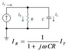
Figure 2: A low pass RC current divider
Figure 2 shows a simple current divider made up of a capacitor and a resistor. Using the formula above, the current in the resistor is given by:


where ZC = 1/(jωC) is the impedance of the capacitor.
The product τ = CR is known as the time constant of the circuit, and the frequency for which ωCR = 1 is called the corner frequency of the circuit. Because the capacitor has zero impedance at high frequencies and infinite impedance at low frequencies, the current in the resistor remains at its DC value IT for frequencies up to the corner frequency, whereupon it drops toward zero for higher frequencies as the capacitor effectively short-circuits the resistor. In other words, the current divider is a low pass filter for current in the resistor.
Loading effect

Figure 3: A current amplifier (gray box) driven by a Norton source (
iS,
RS) and with a resistor load
RL. Current divider in blue box at input (
RS,
Rin) reduces the current gain, as does the current divider in green box at the output (
Rout,
RL)
The gain of an amplifier generally depends on its source and load terminations. Current amplifiers and transconductance amplifiers are characterized by a short-circuit output condition, and current amplifiers and transresistance amplifiers are characterized using ideal infinite impedance current sources. When an amplifier is terminated by a finite, non-zero termination, and/or driven by a non-ideal source, the effective gain is reduced due to the loading effect at the output and/or the input, which can be understood in terms of current division.
Figure 3 shows a current amplifier example. The amplifier (gray box) has input resistance Rin and output resistance Rout and an ideal current gain Ai. With an ideal current driver (infinite Norton resistance) all the source current iS becomes input current to the amplifier. However, for a Norton driver a current divider is formed at the input that reduces the input current to

which clearly is less than iS. Likewise, for a short circuit at the output, the amplifier delivers an output current io = Ai ii to the short-circuit. However, when the load is a non-zero resistor RL, the current delivered to the load is reduced by current division to the value:

Combining these results, the ideal current gain Ai realized with an ideal driver and a short-circuit load is reduced to the loaded gain Aloaded:


The resistor ratios in the above expression are called the loading factors. For more discussion of loading in other amplifier types, see loading effect.
Unilateral versus bilateral amplifiers
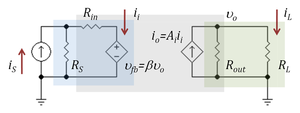
Figure 4: Current amplifier as a bilateral two-port network; feedback through dependent voltage source of gain β V/V
Figure 3 and the associated discussion refers to a unilateral amplifier. In a more general case where the amplifier is represented by a two port, the input resistance of the amplifier depends on its load, and the output resistance on the source impedance. The loading factors in these cases must employ the true amplifier impedances including these bilateral effects. For example, taking the unilateral current amplifier of Figure 3, the corresponding bilateral two-port network is shown in Figure 4 based upon h-parameters.[1] Carrying out the analysis for this circuit, the current gain with feedback Afb is found to be

That is, the ideal current gain Ai is reduced not only by the loading factors, but due to the bilateral nature of the two-port by an additional factor[2] ( 1 + β (RL / RS ) Aloaded ), which is typical of negative feedback amplifier circuits. The factor β (RL / RS ) is the current feedback provided by the voltage feedback source of voltage gain β V/V. For instance, for an ideal current source with RS = ∞ Ω, the voltage feedback has no influence, and for RL = 0 Ω, there is zero load voltage, again disabling the feedback.
References and notes
- ↑ >The h-parameter two port is the only two-port among the four standard choices that has a current-controlled current source on the output side.
- ↑ Often called the improvement factor or the desensitivity factor.


