imported>John R. Brews |
|
| (146 intermediate revisions by one other user not shown) |
| Line 1: |
Line 1: |
| | {{AccountNotLive}} |
| {{TOC|right}} | | {{TOC|right}} |
| A '''current mirror''' is a circuit designed to copy a [[current (electricity)|current]] through one [[active device]] by controlling the current in another active device of a circuit, keeping the output current constant regardless of loading. The current being 'copied' can be, and sometimes is, a varying signal current. Conceptually, an ideal current mirror is simply an ideal current amplifier. The current mirror is used to provide bias currents and [[active load]]s to circuits.
| | [[Image:Current division example.svg|thumbnail|250px|Figure 1: Schematic of an electrical circuit illustrating current division. Notation ''R<sub>T<sub>.</sub></sub>'' refers to the ''total'' resistance of the circuit to the right of resistor ''R<sub>X</sub>''.]] |
|
| |
|
| ==Mirror characteristics==
| | In [[electronics]], a '''current divider ''' is a simple [[linear]] [[Electrical network|circuit]] that produces an output [[Electric current|current]] (''I''<sub>X</sub>) that is a fraction of its input current (''I''<sub>T</sub>). The splitting of current between the branches of the divider is called '''current division'''. The currents in the various branches of such a circuit divide in such a way as to minimize the total energy expended. |
| There are three main specifications that characterize a current mirror. The first is the current level it produces. The second is its AC output resistance, which determines how much the output current varies with the voltage applied to the mirror. The third specification is the minimum voltage drop across the mirror necessary to make it work properly. This minimum voltage is dictated by the need to keep the output transistor of the mirror in active mode. The range of voltages where the mirror works is called the '''compliance range''' and the voltage marking the boundary between good and bad behavior is called the '''compliance voltage'''. There are also a number of secondary performance issues with mirrors, for example, temperature stability.
| |
|
| |
|
| ==Practical approximations==
| | The formula describing a current divider is similar in form to that for the [[voltage divider]]. However, the ratio describing current division places the impedance of the unconsidered branches in the [[numerator]], unlike voltage division where the considered impedance is in the numerator. To be specific, if two or more [[Electrical impedance|impedance]]s are in parallel, the current that enters the combination will be split between them in inverse proportion to their impedances (according to [[Ohm's law]]). It also follows that if the impedances have the same value the current is split equally. |
| For small-signal analysis the current mirror can be approximated by its equivalent [[Norton's theorem| Norton impedance]] .
| |
|
| |
|
| In large-signal hand analysis, a current mirror usually is approximated simply by an ideal current source. However, an ideal current source is unrealistic in several respects:
| | ==Resistive divider== |
| *it has infinite AC impedance, while a practical mirror has finite impedance
| | A general formula for the current ''I<sub>X</sub>'' in a resistor ''R<sub>X</sub>'' that is in parallel with a combination of other resistors of total resistance ''R<sub>T</sub>'' is (see Figure 1): |
| *it provides the same current regardless of voltage, that is, there are no compliance range requirements
| | :<math>I_X = \frac{R_T}{R_X+R_T}I_T \ </math> |
| *it has no frequency limitations, while a real mirror has limitations due to the parasitic capacitances of the transistors
| | where ''I<sub>T</sub>'' is the total current entering the combined network of ''R<sub>X</sub>'' in parallel with ''R<sub>T</sub>''. Notice that when ''R<sub>T</sub>'' is composed of a [[Series_and_parallel_circuits#Parallel_circuits|parallel combination]] of resistors, say ''R<sub>1</sub>'', ''R<sub>2</sub>'', ... ''etc.'', then the reciprocal of each resistor must be added to find the total resistance ''R<sub>T</sub>'': |
| *the ideal source has no sensitivity to real-world effects like noise, power-supply voltage variations and component tolerances.
| | :<math> \frac {1}{R_T} = \frac {1} {R_1} + \frac {1} {R_2} + \frac {1}{R_3} + ... \ . </math> |
|
| |
|
| == Circuit realizations of current mirrors == | | ==General case== |
| {{Image|Simple bipolar mirror.PNG|right|250px|A current mirror implemented with npn bipolar transistors using a resistor to set the reference current I<sub>REF</sub>; V<sub>CC</sub> = supply voltage.}}
| | Although the resistive divider is most common, the current divider may be made of frequency dependent [[Electrical impedance|impedance]]s. In the general case the current I<sub>X</sub> is given by: |
| | :<math>I_X = \frac{Z_T} {Z_X+Z_T}I_T \ ,</math> |
|
| |
|
| ===Basic bipolar transistor mirror=== | | ==Using Admittance== |
| The simplest bipolar current mirror consists of two transistors connected as shown in the figure. Transistor Q<sub>1</sub> is connected so its collector-base voltage is zero. Consequently, the voltage drop across Q<sub>1</sub> is ''V''<sub>BE</sub>, that is, this voltage is set by the [[Diode_modelling#Shockley_diode_model| diode law]] and Q<sub>1</sub> is said to be '''diode connected'''. (See also [[Bipolar_transistor#Ebers.E2.80.93Moll_model|Ebers-Moll model]].) It is important to have Q<sub>1</sub> in the circuit instead of a simple diode, because Q<sub>1</sub> sets ''V<sub>BE</sub>'' for the transistor Q<sub>2</sub>. If Q<sub>1</sub> and Q<sub>2</sub> are matched, that is, have substantially the same device properties, and if the mirror output voltage is chosen so the collector-base voltage of Q<sub>2</sub> also is zero, then the ''V<sub>BE</sub>''-value set by Q<sub>1</sub> results in an emitter current in the matched Q<sub>2</sub> that is the same as the emitter current in Q<sub>1</sub>. Because Q<sub>1</sub> and Q<sub>2</sub> are matched, their β<sub>0</sub>-values also agree, making the mirror output current the same as the collector current of Q<sub>1</sub>.
| | Instead of using [[Electrical impedance|impedance]]s, the current divider rule can be applied just like the [[voltage divider]] rule if [[admittance]] (the inverse of impedance) is used. |
| The current delivered by the mirror for arbitrary collector-base reverse bias ''V''<sub>CB</sub> of the output transistor is given by (see [[bipolar transistor]]):
| | :<math>I_X = \frac{Y_X} {Y_{Total}}I_T</math> |
| | Take care to note that Y<sub>Total</sub> is a straightforward addition, not the sum of the inverses inverted (as you would do for a standard parallel resistive network). For Figure 1, the current I<sub>X</sub> would be |
| | :<math>I_X = \frac{Y_X} {Y_{Total}}I_T = \frac{\frac{1}{R_X}} {\frac{1}{R_X} + \frac{1}{R_1} + \frac{1}{R_2} + \frac{1}{R_3}}I_T</math> |
|
| |
|
| ::<math> I_\mathrm{C} = I_\mathrm{S} \left( e^{\frac{V_\mathrm{BE}}{V_\mathrm{T}}}-1 \right) \left(1 + \begin{matrix} \frac{V_\mathrm{CB}}{V_\mathrm{A}} \end{matrix} \right) </math>, | | ===Example: RC combination=== |
| where ''V<sub>T</sub>'' = [[Boltzmann constant#Role in semiconductor physics: the thermal voltage|thermal voltage]], ''I<sub>S</sub>'' = reverse saturation current, or scale current; ''V<sub>A</sub>'' = [[Early voltage]]. This current is related to the reference current ''I<sub>REF</sub>'' when the output transistor ''V<sub>CB</sub>'' = 0 V by:
| | [[Image:Low pass RC filter.PNG|thumbnail|220px|Figure 2: A low pass RC current divider]] |
| | Figure 2 shows a simple current divider made up of a [[capacitor]] and a resistor. Using the formula above, the current in the resistor is given by: |
|
| |
|
| ::<math> I_{REF} = I_C \left( 1+ \frac {2} {\beta_0} \right) \ , </math> | | ::<math> I_R = \frac {\frac{1}{j \omega C}} {R + \frac{1}{j \omega C} }I_T </math> |
| | :::<math> = \frac {1} {1+j \omega CR} I_T \ , </math> |
| | where ''Z<sub>C</sub> = 1/(jωC) '' is the impedance of the capacitor. |
|
| |
|
| as found using [[Kirchhoff's current law]] at the collector node of Q<sub>1</sub>. The reference current supplies the collector current to Q<sub>1</sub> and the base currents to both transistors — when both transistors have zero base-collector bias, the two base currents are equal. Parameter β<sub>0</sub> is the transistor β-value for ''V''<sub>CB</sub> = 0 V. | | The product ''τ = CR'' is known as the [[time constant]] of the circuit, and the frequency for which ωCR = 1 is called the [[corner frequency]] of the circuit. Because the capacitor has zero impedance at high frequencies and infinite impedance at low frequencies, the current in the resistor remains at its DC value ''I<sub>T</sub>'' for frequencies up to the corner frequency, whereupon it drops toward zero for higher frequencies as the capacitor effectively [[short-circuit]]s the resistor. In other words, the current divider is a [[low pass filter]] for current in the resistor. |
|
| |
|
| ====Output resistance==== | | ==Loading effect== |
| If V<sub>CB</sub> is greater than zero in output transistor Q<sub>2</sub>, the collector current in Q<sub>2</sub> will be somewhat larger than for Q<sub>1</sub> due to the [[Early effect]]. In other words, the mirror has a finite output (or Norton) resistance given by the ''r<sub>O</sub>'' of the output transistor, namely (see [[Early effect]]):
| | [[Image:Current division.PNG|thumbnail|300px|Figure 3: A current amplifier (gray box) driven by a Norton source (''i<sub>S</sub>'', ''R<sub>S</sub>'') and with a resistor load ''R<sub>L</sub>''. Current divider in blue box at input (''R<sub>S</sub>'',''R<sub>in</sub>'') reduces the current gain, as does the current divider in green box at the output (''R<sub>out</sub>'',''R<sub>L</sub>'')]] |
| | The gain of an amplifier generally depends on its source and load terminations. Current amplifiers and transconductance amplifiers are characterized by a short-circuit output condition, and current amplifiers and transresistance amplifiers are characterized using ideal infinite impedance current sources. When an amplifier is terminated by a finite, non-zero termination, and/or driven by a non-ideal source, the effective gain is reduced due to the '''loading effect''' at the output and/or the input, which can be understood in terms of current division. |
|
| |
|
| ::<math> R_N =r_O = \begin{matrix} \frac {V_A + V_{CB}} {I_C} \end{matrix} </math>,
| | Figure 3 shows a current amplifier example. The amplifier (gray box) has input resistance ''R<sub>in</sub>'' and output resistance ''R<sub>out</sub>'' and an ideal current gain ''A<sub>i</sub>''. With an ideal current driver (infinite Norton resistance) all the source current ''i<sub>S</sub>'' becomes input current to the amplifier. However, for a [[Norton's theorem|Norton driver]] a current divider is formed at the input that reduces the input current to |
|
| |
|
| where ''V<sub>A</sub>'' = Early voltage and ''V<sub>CB</sub>'' = collector-to-base bias.
| | ::<math>i_{i} = \frac {R_S} {R_S+R_{in}} i_S \ , </math> |
| ====Compliance voltage====
| |
| To keep the output transistor active, ''V<sub>CB</sub>'' ≥ 0 V. That means the lowest output voltage that results in correct mirror behavior, the compliance voltage, is ''V<sub>OUT</sub>'' = ''V<sub>CV</sub>'' = ''V<sub>BE</sub>'' under bias conditions with the output transistor at the output current level ''I<sub>C</sub>'' and with ''V<sub>CB</sub>'' = 0 V or, inverting the ''I-V'' relation above:
| |
|
| |
|
| ::<math>\ V_{CV}= {V_T}</math> <math>\ \mathrm {ln} </math> <math> \left(\begin{matrix}\frac {I_C}{I_S}\end{matrix}+1\right) \ , </math>
| | which clearly is less than ''i<sub>S</sub>''. Likewise, for a short circuit at the output, the amplifier delivers an output current ''i<sub>o</sub>'' = ''A<sub>i</sub> i<sub>i</sub>'' to the short-circuit. However, when the load is a non-zero resistor ''R<sub>L</sub>'', the current delivered to the load is reduced by current division to the value: |
|
| |
|
| where ''V<sub>T</sub>'' = [[Boltzmann constant#Role in semiconductor physics: the thermal voltage|thermal voltage]] and ''I<sub>S</sub>'' = reverse saturation current (scale current).
| | ::<math>i_L = \frac {R_{out}} {R_{out}+R_{L}} A_i i_{i} \ . </math> |
|
| |
|
| ====Extensions and complications====
| | Combining these results, the ideal current gain ''A<sub>i</sub>'' realized with an ideal driver and a short-circuit load is reduced to the '''loaded gain''' ''A<sub>loaded</sub>'': |
| When Q<sub>2</sub> has ''V<sub>CB</sub>'' > 0 V, the transistors no longer are matched. In particular, their β-values differ due to the Early effect, with
| |
| ::<math>{\beta}_1 = {\beta}_{0} \ \operatorname{and} \ {\beta}_2 = {\beta}_{0}\ (1 + \frac{V_{CB}}{V_A})</math>
| |
| where V<sub>A</sub> is the [[Early effect|Early voltage]] and β<sub>0</sub> = transistor β for V<sub>CB</sub> = 0 V. Besides the difference due to the Early effect, the transistor β-values will differ because the β<sub>0</sub>-values depend on current, and the two transistors now carry different currents (see [[Gummel–Poon model|Gummel-Poon model]]).
| |
|
| |
|
| Further, Q<sub>2</sub> may get substantially hotter than Q<sub>1</sub> due to the associated higher power dissipation. To maintain matching, the temperature of the transistors must be nearly the same. In [[integrated circuit]]s and transistor arrays where both transistors are on the same die, this is easy to achieve. But if the two transistors are widely separated, the precision of the current mirror is compromised.
| | ::<math>A_{loaded} =\frac {i_L} {i_S} = \frac {R_S} {R_S+R_{in}}</math> <math> \frac {R_{out}} {R_{out}+R_{L}} A_i \ . </math> |
|
| |
|
| Additional matched transistors can be connected to the same base and will supply the same collector current. In other words, the right half of the circuit can be duplicated several times with various resistor values replacing R<sub>2</sub> on each. Note, however, that each additional right-half transistor "steals" a bit of collector current from Q<sub>1</sub> due to the non-zero base currents of the right-half transistors. This will result in a small reduction in the programmed current.
| | The resistor ratios in the above expression are called the '''loading factors'''. For more discussion of loading in other amplifier types, see [[Voltage division#Loading effect|loading effect]]. |
|
| |
|
| An example of a mirror with emitter degeneration to increase mirror resistance is found in [[Two-port network#Impedance parameters (z-parameters)|two-port network]]s.
| | ===Unilateral versus bilateral amplifiers=== |
| | [[Image:H-parameter current amplifier.PNG|thumbnail|300px|Figure 4: Current amplifier as a bilateral two-port network; feedback through dependent voltage source of gain β V/V]] |
| | Figure 3 and the associated discussion refers to a [[Electronic amplifier#Unilateral or bilateral|unilateral]] amplifier. In a more general case where the amplifier is represented by a [[two-port network|two port]], the input resistance of the amplifier depends on its load, and the output resistance on the source impedance. The loading factors in these cases must employ the true amplifier impedances including these bilateral effects. For example, taking the unilateral current amplifier of Figure 3, the corresponding bilateral two-port network is shown in Figure 4 based upon [[Two-port network#Hybrid parameters (h-parameters)| h-parameters]].<ref name=H_port/> Carrying out the analysis for this circuit, the current gain with feedback ''A<sub>fb</sub>'' is found to be |
|
| |
|
| For the simple mirror shown in the diagram, typical values of <math>\beta</math> will yield a current match of 1% or better.
| | ::<math> A_{fb} = \frac {i_L}{i_S} = \frac {A_{loaded}} {1+ {\beta}(R_L/R_S) A_{loaded}} \ . </math> |
|
| |
|
| === Basic MOSFET current mirror ===
| | That is, the ideal current gain ''A<sub>i</sub>'' is reduced not only by the loading factors, but due to the bilateral nature of the two-port by an additional factor<ref>Often called the ''improvement factor'' or the ''desensitivity factor''.</ref> ( 1 + β (R<sub>L</sub> / R<sub>S</sub> ) A<sub>loaded</sub> ), which is typical of [[negative feedback amplifier]] circuits. The factor β (R<sub>L</sub> / R<sub>S</sub> ) is the current feedback provided by the voltage feedback source of voltage gain β V/V. For instance, for an ideal current source with ''R<sub>S</sub>'' = ∞ Ω, the voltage feedback has no influence, and for ''R<sub>L</sub>'' = 0 Ω, there is zero load voltage, again disabling the feedback. |
| {{Image|Simple MOSFET mirror.PNG|right|250px| An n-channel MOSFET current mirror with a resistor to set the reference current I<sub>REF</sub>; V<sub>DD</sub> is the supply voltage.}}
| |
| The basic current mirror can also be implemented using MOSFET transistors, as shown in the adjacent figure. Transistor ''M''<sub>1</sub> is operating in the [[MOSFET#Modes of operation|saturation or active]] mode, and so is ''M''<sub>2</sub>. In this setup, the output current ''I''<sub>OUT</sub> is directly related to ''I''<sub>REF</sub>, as discussed next.
| |
| | |
| The drain current of a MOSFET ''I''<sub>D</sub> is a function of both the gate-source voltage and the drain-to-gate voltage of the MOSFET given by ''I''<sub>D</sub> = ''f'' (''V''<sub>GS</sub>, ''V''<sub>DG</sub>), a relationship derived from the functionality of the [[MOSFET]] device. In the case of transistor ''M''<sub>1</sub> of the mirror, ''I''<sub>D</sub> = ''I''<sub>REF</sub>. Reference current ''I''<sub>REF</sub> is a known current, and can be provided by a resistor as shown, or by a "threshold-referenced" or "self-biased" current source to insure that it is constant, independent of voltage supply variations.<ref name=Gray-Meyer/>
| |
| | |
| Using ''V''<sub>DG</sub>=0 for transistor ''M''<sub>1</sub>, the drain current in ''M''<sub>1</sub> is ''I''<sub>D</sub> = ''f'' (''V''<sub>GS</sub>,''V''<sub>DG</sub>=0), so we find: ''f'' (''V''<sub>GS</sub>, 0) = ''I''<sub>REF</sub>, implicitly determining the value of ''V''<sub>GS</sub>. Thus ''I''<sub>REF</sub> sets the value of ''V''<sub>GS</sub>. The circuit in the diagram forces the same ''V''<sub>GS</sub> to apply to transistor ''M''<sub>2</sub>. If ''M''<sub>2</sub> also is biased with zero ''V''<sub>DG</sub> and provided both transistors ''M''<sub>1</sub> and ''M''<sub>2</sub> have good matching of their properties, such as channel length, width, threshold voltage ''etc.'', the relationship ''I''<sub>OUT</sub> = ''f'' (''V''<sub>GS</sub>,''V''<sub>DG</sub>=0 ) applies, thus setting ''I''<sub>OUT</sub> = ''I''<sub>REF</sub>; that is, the output current is the same as the reference current when ''V''<sub>DG</sub>=0 for the output transistor, and both transistors are matched.
| |
| | |
| The drain-to-source voltage can be expressed as ''V''<sub>DS</sub>=''V''<sub>DG</sub> +''V''<sub>GS</sub>. With this substitution, the Shichman-Hodges model provides an approximate form for function ''f'' (''V''<sub>GS</sub>,''V''<sub>DG</sub>):<ref name=Gray-Meyer2/>
| |
| | |
| :::<math>
| |
| \begin{alignat}{2}
| |
| I_{d} & = f\ (V_{GS},V_{DG})
| |
| = \begin{matrix} \frac{1}{2}K_{p}\left(\frac{W}{L}\right)\end{matrix}(V_{GS} - V_{th})^2 (1 + \lambda V_{DS}) \\
| |
| & =\begin{matrix} \frac{1}{2}K_{p}\left(\frac{W}{L}\right)\end{matrix}(V_{GS} - V_{th})^2 \left( 1 + \lambda (V_{DG}+V_{GS}) \right) \\
| |
| \end{alignat}</math>
| |
| | |
| where, <math>{K_{p}}</math> is a technology related constant associated with the transistor, ''W/L'' is the width to length ratio of the transistor, ''V''<sub>GS</sub> is the gate-source voltage, ''V''<sub>th</sub> is the threshold voltage, λ is the [[channel length modulation]] constant, and ''V''<sub>DS</sub> is the drain source voltage.
| |
| ====Output resistance====
| |
| Because of channel-length modulation, the mirror has a finite output (or Norton) resistance given by the ''r<sub>O</sub>'' of the output transistor, namely (see [[channel length modulation]]):
| |
| | |
| ::<math> R_N =r_O = \begin{matrix} \frac {1/\lambda + V_{DS}} {I_D} \end{matrix} </math>,
| |
| | |
| where ''λ'' = channel-length modulation parameter and ''V<sub>DS</sub>'' = drain-to-source bias.
| |
| ====Compliance voltage====
| |
| To keep the output transistor resistance high, ''V<sub>DG</sub>'' ≥ 0 V.<ref name=Note1/> See Baker. <ref name=Baker/> That means the lowest output voltage that results in correct mirror behavior, the compliance voltage, is ''V<sub>OUT</sub>'' = ''V<sub>CV</sub>'' = ''V<sub>GS</sub>'' for the output transistor at the output current level with ''V<sub>DG</sub>'' = 0 V, or using the inverse of the ''f''-function, ''f<sup> −1</sup>'':
| |
| | |
| ::<math> V_{CV}= V_{GS} (\mathrm{for}\ I_D\ \mathrm{at} \ V_{DG}=0V) = f ^{-1} (I_D) \ \mathrm{with}\ V_{DG}=0 </math>.
| |
| | |
| For Shichman-Hodges model, ''f<sup> -1</sup>'' is approximately a square-root function.
| |
| | |
| ====Extensions and reservations====
| |
| | |
| A useful feature of this mirror is the linear dependence of ''f'' upon device width ''W'', a proportionality approximately satisfied even for models more accurate than the Shichman-Hodges model. Thus, by adjusting the ratio of widths of the two transistors, multiples of the reference current can be generated.
| |
| | |
| It must be recognized that the Shichman-Hodges model<ref name=NanoDotTek/> is accurate only for rather dated technology, although it often is used simply for convenience even today. Any quantitative design based upon new technology uses computer models for the devices that account for the changed current-voltage characteristics. Among the differences that must be accounted for in an accurate design is the failure of the square law in ''V''<sub>gs</sub> for voltage dependence and the very poor modeling of ''V''<sub>ds</sub> drain voltage dependence provided by λ''V''<sub>ds</sub>. Another failure of the equations that proves very significant is the inaccurate dependence upon the channel length ''L''. A significant source of ''L''-dependence stems from λ, as noted by Gray and Meyer, who also note that λ usually must be taken from experimental data.<ref name=Gray-Meyer3/>
| |
| | |
| ===Feedback assisted current mirror===
| |
| {{Image|Gain-assisted current mirror.PNG|right|350px| Gain-boosted current mirror with op amp feedback to increase output resistance.}}
| |
| {{Image|Wide-swing MOSFET mirror.PNG|right|350px| MOSFET version of wide-swing current mirror; M<sub>1</sub> and M<sub>2</sub> are in active mode, while M<sub>3</sub> and M<sub>4</sub> are in Ohmic mode and act like resistors.}}
| |
| Figure 3 shows a mirror using [[negative feedback]] to increase output resistance. Because of the op amp, these circuits are sometimes called '''gain-boosted current mirrors'''. Because they have relatively low compliance voltages, they also are called '''wide-swing current mirrors'''. A variety of circuits based upon this idea are in use,<ref name=Baker2/><ref name=Ivanov/><ref name=Sansen/> particularly for MOSFET mirrors because MOSFETs have rather low intrinsic output resistance values. A MOSFET version of Figure 3 is shown in Figure 4 where MOSFETs ''M<sub>3</sub>'' and ''M<sub>4</sub>'' operate in [[MOSFET#Modes_of_operation|Ohmic mode]] to play the same role as emitter resistors ''R<sub>E</sub>'' in Figure 3, and MOSFETs ''M<sub>3</sub>'' and ''M<sub>4</sub>'' operate in active mode in the same roles as mirror transistors ''Q<sub>1</sub>'' and ''Q<sub>2</sub>'' in Figure 3. An explanation follows of how the circuit in Figure 3 works.
| |
| | |
| The operational amplifier is fed the difference in voltages ''V<sub>1</sub> - V<sub>2</sub>'' at the top of the two emitter-leg resistors of value ''R<sub>E</sub>''. This difference is amplified by the op amp and fed to the base of output transistor ''Q<sub>2</sub>''. If the collector base reverse bias on ''Q<sub>2</sub>'' is increased by increasing the applied voltage ''V<sub>A</sub>'', the current in ''Q<sub>2</sub>'' increases, increasing ''V<sub>2</sub>'' and decreasing the difference ''V<sub>1</sub> - V<sub>2</sub>'' entering the op amp. Consequently, the base voltage of ''Q<sub>2</sub>'' is decreased, and ''V<sub>BE</sub>'' of ''Q<sub>2</sub>'' decreases, counteracting the increase in output current.
| |
| | |
| If the op amp gain ''A<sub>v</sub>'' is large, only a very small difference ''V<sub>1</sub> - V<sub>2</sub>'' is sufficient to generate the needed base voltage ''V<sub>B</sub>'' for ''Q<sub>2</sub>'', namely
| |
| ::<math> V_1-V_2 = \frac {V_B}{A_v} \ .</math>
| |
| Consequently, the currents in the two leg resistors are held nearly the same, and the output current of the mirror is very nearly the same as the collector current ''I<sub>C1</sub>'' in ''Q<sub>1</sub>'', which in turn is set by the reference current as
| |
| ::<math> I_{ref} = I_{C1} (1 + 1/ { \beta}_1) \ ,</math>
| |
| where β<sub>1</sub> for transistor ''Q<sub>1</sub>'' and β<sub>2</sub> for ''Q<sub>2</sub>'' differ due to the [[Early effect]] if the reverse bias across the collector-base of ''Q<sub>2</sub>'' is non-zero.
| |
| | |
| {{Image|Mirror output resistance.PNG|right|350px|Small-signal circuit to determine output resistance of mirror; transistor Q<sub>2</sub> is replaced with its [[hybrid-pi model]]; a test current ''I''<sub>X</sub> at the output generates a voltage ''V''<sub>X</sub>, and the output resistance is ''R''<sub>out</sub><nowiki> = </nowiki>''V''<sub>X</sub> / ''I''<sub>X</sub>.}}
| |
| | |
| ====Output resistance====
| |
| An idealized treatment of output resistance is given in the footnote.<ref name=outputR/> A small-signal analysis for an op amp with finite gain ''A''<sub>v</sub> but otherwise ideal is based upon Figure 5 (β, r<sub>O</sub> and ''r<sub>π</sub>'' refer to ''Q<sub>2</sub>''). To arrive at Figure 5, notice that the positive input of the op amp in Figure 3 is at AC ground, so the voltage input to the op amp is simply the AC emitter voltage ''V''<sub>e</sub> applied to its negative input, resulting in a voltage output of −''A''<sub>v</sub> ''V''<sub>e</sub>. Using [[Ohm's law]] across the input resistance r<sub>π</sub> determines the small-signal base current ''I''<sub>b</sub> as:
| |
| | |
| :<math> I_b = \frac {V_e} {r_{\pi} / ( A_v+1) } \ . </math>
| |
| | |
| Combining this result with Ohm's law for ''R''<sub>E</sub>, ''V''<sub>e</sub> can be eliminated, to find:<ref name=limit/>
| |
| | |
| :<math> I_b = I_X \frac {R_E} {R_E +\frac {r_{\pi}} {A_v+1} } \ . </math>
| |
| | |
| [[Kirchhoff's voltage law]] from the test source ''I''<sub>X</sub> to the ground of ''R''<sub>E</sub> provides:
| |
| | |
| :<math> V_X = (I_X + \beta I_b) r_O + (I_X - I_b )R_E \ . </math>
| |
| | |
| Substituting for ''I''<sub>b</sub> and collecting terms the output resistance ''R''<sub>out</sub> is found to be:
| |
| | |
| :<math>R_{out} = \frac {V_X} {I_X} = r_O \left( 1+ \beta \frac{R_E} {R_E+r_{\pi}/(A_v+1)} \right) +R_E\|\frac {r_{\pi}} {A_v+1} \ .</math>
| |
| | |
| For a large gain ''A<sub>v</sub> >> r<sub>π</sub> / R<sub>E</sub>'' the maximum output resistance obtained with this circuit is
| |
| ::<math>R_{out} = ( \beta +1) r_O \ ,</math>
| |
| a substantial improvement over the basic mirror where ''R<sub>out</sub> = ''r<sub>O</sub>''.
| |
| | |
| The small-signal analysis of the MOSFET circuit of Figure 4 is obtained from the bipolar analysis by setting β = ''g<sub>m</sub> r<sub>π</sub>'' in the formula for ''R<sub>out</sub>'' and then letting ''r<sub>π</sub>'' → ∞. The result is
| |
| | |
| ::<math>R_{out} = r_O \left( 1+ g_m R_E(A_v+1) \right) +R_E \ .</math>
| |
| | |
| This time, ''R<sub>E</sub>'' is the resistance of the source-leg MOSFETs M<sub>3</sub>, M<sub>4</sub>. Unlike Figure 3, however, as ''A<sub>v</sub>'' is increased (holding ''R<sub>E</sub>'' fixed in value), ''R<sub>out</sub>'' continues to increase, and does not approach a limiting value at large ''A<sub>v</sub>''.
| |
| | |
| ====Compliance voltage====
| |
| For Figure 3, a large op amp gain achieves the maximum ''R<sub>out</sub>'' with only a small ''R<sub>E</sub>''. A low value for ''R<sub>E</sub>'' means ''V<sub>2</sub>'' also is small, allowing a low compliance voltage for this mirror, only a voltage ''V<sub>2</sub>'' larger than the compliance voltage of the simple bipolar mirror. For this reason this type of mirror also is called a ''wide-swing current mirror'', because it allows the output voltage to swing low compared to other types of mirror that achieve a large ''R<sub>out</sub>'' only at the expense of large compliance voltages.
| |
| | |
| With the MOSFET circuit of Figure 4, like the circuit in Figure 3, the larger the op amp gain ''A<sub>v</sub>'', the smaller ''R<sub>E</sub>'' can be made at a given ''R<sub>out</sub>'', and the lower the compliance voltage of the mirror.
| |
| | |
| ===Other current mirrors===
| |
| There are many sophisticated current mirrors that have higher [[output impedance|output resistances]] than the basic mirror (more closely approach an ideal mirror with current output independent of output voltage) and produce currents less sensitive to temperature and device parameter [[Design for manufacturability (IC)|variations]] and to circuit voltage fluctuations. These multi-transistor mirror circuits are used both with bipolar and MOS transistors.
| |
| These circuits include:
| |
| * the [[Widlar current source]]
| |
| * the [[Wilson current source]]
| |
| * the [[Cascode|cascoded current sources]]
| |
| | |
| ==References==
| |
|
| |
|
| | ==References and notes== |
| {{reflist|refs= | | {{reflist|refs= |
|
| |
|
| <ref name=Gray-Meyer> | | <ref name=H_port>>The [[Two-port network#Hybrid parameters (h-parameters)|h-parameter two port]] is the only two-port among the four standard choices that has a current-controlled current source on the output side.</ref> |
| {{cite book
| |
| |author=Paul R. Gray, Paul J. Hurst, Stephen H. Lewis, Robert G. Meyer
| |
| |title=Analysis and Design of Analog Integrated Circuits
| |
| |year= 2001
| |
| |page=pp. 308–309
| |
| |edition=Fourth Edition
| |
| |publisher=Wiley
| |
| |location=New York
| |
| |isbn=0471321680
| |
| |url=http://worldcat.org/isbn/0471321680}}
| |
| </ref>
| |
| | |
| <ref name=Gray-Meyer2>
| |
| {{cite book
| |
| |author=Gray ''et al.''
| |
| |title=Eq. 1.165, p. 44
| |
| |isbn=0471321680
| |
| |url=http://worldcat.org/isbn/0471321680}}
| |
| </ref>
| |
| | |
| <ref name=Note1>Keeping the output resistance high means more than keeping the MOSFET in active mode, because the output resistance of real MOSFETs only begins to increase on entry into the active region, then rising to become close to maximum value only when ''V<sub>DG</sub>'' ≥ 0 V. </ref>
| |
| | |
| <ref name=Baker>
| |
| {{cite book
| |
| |author=R. Jacob Baker
| |
| |title=CMOS Circuit Design, Layout and Simulation
| |
| |edition=Revised Second Edition
| |
| |year= 2008
| |
| |pages=p. 297, §9.2.1 and Figure 20.28, p. 636
| |
| |publisher=Wiley-IEEE
| |
| |location=New York
| |
| |isbn=978-0-470-22941-5
| |
| |url=http://worldcat.org/isbn/0-471-70055-X }}
| |
| </ref>
| |
| | |
| <ref name=NanoDotTek>
| |
| NanoDotTek Report NDT14-08-2007, 12 August 2007 [http://www.nanodottek.com/NDT14_08_2007.pdf]
| |
| </ref>
| |
| | |
| <ref name=Gray-Meyer3>
| |
| {{cite book
| |
| |author=Gray ''et al.''
| |
| |title=p. 44
| |
| |isbn=0471321680
| |
| |url=http://worldcat.org/isbn/0471321680}}
| |
| </ref>
| |
| | |
| <ref name=Baker2>
| |
| {{cite book
| |
| |author=R. Jacob Baker
| |
| |title=§ 20.2.4 pp. 645–646
| |
| |isbn=978-0-470-22941-5
| |
| |url=http://worldcat.org/isbn/0-471-70055-X }}
| |
| </ref>
| |
| | |
| <ref name=Ivanov>
| |
| {{cite book
| |
| |author=Ivanov VI and Filanovksy IM
| |
| |title=Operational amplifier speed and accuracy improvement: analog circuit design with structural methodology | |
| |edition=The Kluwer international series in engineering and computer science, v. 763
| |
| |year= 2004
| |
| |page=§6.1, p. 105-108
| |
| |publisher=Kluwer Academic
| |
| |location=Boston, Mass.
| |
| |isbn=1-4020-7772-6
| |
| |url=http://books.google.com/books?id=IuLsny9wKIIC&pg=PA110&dq=gain+boost+wide++%22current+mirror%22&lr=&as_brr=0&sig=bnTLU_pFGG82g9N5x3urxIPqCzA#PPA107,M1}}
| |
| </ref>
| |
| | |
| <ref name=Sansen>
| |
| {{cite book
| |
| |author=W. M. C. Sansen
| |
| |title=Analog design essentials
| |
| |year= 2006
| |
| |page=§0310, p. 93
| |
| |publisher=Springer
| |
| |location=New York ; Berlin
| |
| |isbn=0-387-25746-2
| |
| |url=http://worldcat.org/isbn/0387257462}}
| |
| </ref>
| |
| | |
| <ref name=outputR>An idealized version of the argument in the text, valid for infinite op amp gain, is as follows. If the op amp is replaced by a [[nullor]], voltage ''V''<sub>2</sub> = ''V''<sub>1</sub>, so the currents in the leg resistors are held at the same value. That means the emitter currents of the transistors are the same. If the ''V''<sub>CB</sub> of Q<sub>2</sub> increases, so does the output transistor β because of the [[Early effect]]: β = β<sub>0</sub> ( 1 + ''V''<sub>CB</sub> / ''V''<sub>A</sub> ). Consequently the base current to Q<sub>2</sub> given by ''I''<sub>B</sub> = ''I''<sub>E</sub> / (β + 1) decreases and the output current ''I''<sub>out</sub> = ''I''<sub>E</sub> / (1 + 1 / β) increases slightly because β increases slightly. Doing the math,
| |
|
| |
| ::<math> \frac {1} {R_{out}} = \frac {\partial I_{out} } { \partial V_{CB} } = I_E \frac {\partial } { \partial V_{CB} } \left( \frac { \beta } { \beta +1} \right) = I_E \frac {1} {(\beta + 1)^2 } \frac { \partial \beta } {\partial V_{CB}} </math>   <math> = \frac {\beta I_E} { \beta +1 } \frac {1}{\beta} \frac {\beta_0} { V_A} \frac {1} {(\beta +1) }
| |
| | |
| =I_{out} \frac {1} {1+V_{CB} / V_A} \frac {1} { V_A} \frac {1} {(\beta +1) }
| |
| | |
| = \frac {1} { ( \beta +1 ) r_0} \ ,</math>
| |
| | |
| where the transistor output resistance is given by r<sub>O</sub> = ( ''V''<sub>A</sub> + ''V''<sub>CB</sub> ) / ''I''<sub>out</sub>. That is, the ideal mirror resistance for the circuit using an ideal op amp [[nullor]] is ''R''<sub>out</sub> = ( β + 1 ) r<sub>O</sub>, in agreement with the value given later in the text when the gain → ∞.</ref>
| |
| | |
| <ref name=limit>Notice that as ''A''<sub>v</sub> → ∞, ''V''<sub>e</sub> → 0 and ''I''<sub>b</sub> → ''I<sub>X</sub>.</ref>
| |
|
| |
|
| }} | | }} |
The account of this former contributor was not re-activated after the server upgrade of March 2022.

Figure 1: Schematic of an electrical circuit illustrating current division. Notation
RT. refers to the
total resistance of the circuit to the right of resistor
RX.
In electronics, a current divider is a simple linear circuit that produces an output current (IX) that is a fraction of its input current (IT). The splitting of current between the branches of the divider is called current division. The currents in the various branches of such a circuit divide in such a way as to minimize the total energy expended.
The formula describing a current divider is similar in form to that for the voltage divider. However, the ratio describing current division places the impedance of the unconsidered branches in the numerator, unlike voltage division where the considered impedance is in the numerator. To be specific, if two or more impedances are in parallel, the current that enters the combination will be split between them in inverse proportion to their impedances (according to Ohm's law). It also follows that if the impedances have the same value the current is split equally.
Resistive divider
A general formula for the current IX in a resistor RX that is in parallel with a combination of other resistors of total resistance RT is (see Figure 1):

where IT is the total current entering the combined network of RX in parallel with RT. Notice that when RT is composed of a parallel combination of resistors, say R1, R2, ... etc., then the reciprocal of each resistor must be added to find the total resistance RT:

General case
Although the resistive divider is most common, the current divider may be made of frequency dependent impedances. In the general case the current IX is given by:

Using Admittance
Instead of using impedances, the current divider rule can be applied just like the voltage divider rule if admittance (the inverse of impedance) is used.

Take care to note that YTotal is a straightforward addition, not the sum of the inverses inverted (as you would do for a standard parallel resistive network). For Figure 1, the current IX would be

Example: RC combination
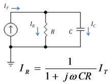
Figure 2: A low pass RC current divider
Figure 2 shows a simple current divider made up of a capacitor and a resistor. Using the formula above, the current in the resistor is given by:


where ZC = 1/(jωC) is the impedance of the capacitor.
The product τ = CR is known as the time constant of the circuit, and the frequency for which ωCR = 1 is called the corner frequency of the circuit. Because the capacitor has zero impedance at high frequencies and infinite impedance at low frequencies, the current in the resistor remains at its DC value IT for frequencies up to the corner frequency, whereupon it drops toward zero for higher frequencies as the capacitor effectively short-circuits the resistor. In other words, the current divider is a low pass filter for current in the resistor.
Loading effect

Figure 3: A current amplifier (gray box) driven by a Norton source (
iS,
RS) and with a resistor load
RL. Current divider in blue box at input (
RS,
Rin) reduces the current gain, as does the current divider in green box at the output (
Rout,
RL)
The gain of an amplifier generally depends on its source and load terminations. Current amplifiers and transconductance amplifiers are characterized by a short-circuit output condition, and current amplifiers and transresistance amplifiers are characterized using ideal infinite impedance current sources. When an amplifier is terminated by a finite, non-zero termination, and/or driven by a non-ideal source, the effective gain is reduced due to the loading effect at the output and/or the input, which can be understood in terms of current division.
Figure 3 shows a current amplifier example. The amplifier (gray box) has input resistance Rin and output resistance Rout and an ideal current gain Ai. With an ideal current driver (infinite Norton resistance) all the source current iS becomes input current to the amplifier. However, for a Norton driver a current divider is formed at the input that reduces the input current to

which clearly is less than iS. Likewise, for a short circuit at the output, the amplifier delivers an output current io = Ai ii to the short-circuit. However, when the load is a non-zero resistor RL, the current delivered to the load is reduced by current division to the value:

Combining these results, the ideal current gain Ai realized with an ideal driver and a short-circuit load is reduced to the loaded gain Aloaded:


The resistor ratios in the above expression are called the loading factors. For more discussion of loading in other amplifier types, see loading effect.
Unilateral versus bilateral amplifiers
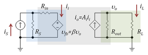
Figure 4: Current amplifier as a bilateral two-port network; feedback through dependent voltage source of gain β V/V
Figure 3 and the associated discussion refers to a unilateral amplifier. In a more general case where the amplifier is represented by a two port, the input resistance of the amplifier depends on its load, and the output resistance on the source impedance. The loading factors in these cases must employ the true amplifier impedances including these bilateral effects. For example, taking the unilateral current amplifier of Figure 3, the corresponding bilateral two-port network is shown in Figure 4 based upon h-parameters.[1] Carrying out the analysis for this circuit, the current gain with feedback Afb is found to be

That is, the ideal current gain Ai is reduced not only by the loading factors, but due to the bilateral nature of the two-port by an additional factor[2] ( 1 + β (RL / RS ) Aloaded ), which is typical of negative feedback amplifier circuits. The factor β (RL / RS ) is the current feedback provided by the voltage feedback source of voltage gain β V/V. For instance, for an ideal current source with RS = ∞ Ω, the voltage feedback has no influence, and for RL = 0 Ω, there is zero load voltage, again disabling the feedback.
References and notes
- ↑ >The h-parameter two port is the only two-port among the four standard choices that has a current-controlled current source on the output side.
- ↑ Often called the improvement factor or the desensitivity factor.


