imported>John R. Brews |
imported>John R. Brews |
| Line 43: |
Line 43: |
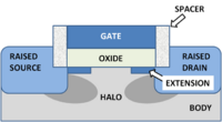
| |MOSFET junction structure.PNG|A modern MOSFET | | |MOSFET junction structure.PNG|A modern MOSFET |
| |Silicon density of states.PNG|Calculated density of states for crystalline silicon. | | |Silicon density of states.PNG|Calculated density of states for crystalline silicon. |
| |Seimiconductor band bending.PNG|A narrow, surface inversion layer of electrons forms at large enough positive gate voltages. The horizontal dashed line indicates the [[Fermi level]] that divides occupied energy levels from empty ones at zero temperature. | | |Seimiconductor band bending.PNG|''Filed effect'': A narrow, surface inversion layer of electrons forms at a semiconductor surface in response to a gate voltage above threshold. |
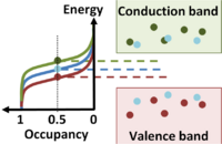
| |Fermi levels.PNG|Occupancy comparison between n-type, intrinsic and p-type semiconductors. | | |Fermi levels.PNG|Occupancy comparison between n-type, intrinsic and p-type semiconductors. |
| }} | | }} |
Revision as of 12:22, 8 January 2011
I am a Professor Emeritus of Electrical Engineering from The University of Arizona, where I taught device physics and circuit design for just under two decades. Previously, I was a research scientist for twenty-odd years at Bell Laboratories, Murray Hill, doing theoretical work in the areas of solid-state physics and device physics. I also am a Fellow of the IEEE, and a recipient of the Electron Device Society distinguished service award for work as Editor-in-chief of the journal IEEE Electron Device Letters, founded by Nobel prize winner George E. Smith. I've published a number of technical books and papers, some of which may be found at this link.
Images
| Magnetism
|
|
|
(CC) Image: John R. Brews
|
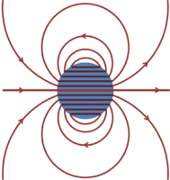
B-field lines near uniformly magnetized sphere
|
|
|
(CC) Image: John R. Brews
|
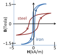
Magnetic flux density vs. magnetic field in steel and iron
|
|
| Widlar current source
|
|
|
(CC) Image: John R. Brews
|
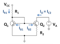
Widlar current source using bipolar transistors
|
|
|
(CC) Image: John R. Brews
|
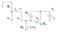
Small-signal circuit for finding output resistance of the Widlar source
|
|
|
(CC) Image: John R. Brews
|
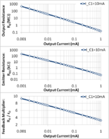
Design trade-off between output resistance and output current in Widlar source
|
|
| Forces
|
|
|
(CC) Image: John R. Brews
|
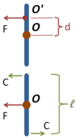
Force and its equivalent force and couple
|
|
| Electromagnetism
|
|
|
(CC) Image: John R. Brews
|
|
|
|
| Devices
|
|
|
(PD) Image: John R. Brews
|
A modern MOSFET
|
|
|
(CC) Image: John R. Brews
|
Calculated density of states for crystalline silicon.
|
|
|
(CC) Image: John R. Brews
|
Filed effect: A narrow, surface inversion layer of electrons forms at a semiconductor surface in response to a gate voltage above threshold.
|
|
|
(PD) Image: John R. Brews
|
Occupancy comparison between n-type, intrinsic and p-type semiconductors.
|
|
